
Altium Standards
This guide is a cheatsheet of what I think are the most useful part of a more formal standard I wrote here.
Schematic
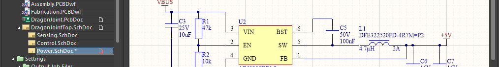
- Power port naming:
- Power ports of specific value shall be named:
- {type}{polarity}{value}V
- Power ports of variable value shall be named:
- V{name}{polarity}
- Ground/Common ports shall be named:
- {type}GND
- Power ports of specific value shall be named:
- {type} (is optional) denotes the power port type (eg, ANA for analog).
- {polarity} is either + or -
- {value} is a numeric value, use decimals if necessary
- {name} is a descriptive name of a port
| ANA+5.5V | VUSB+ | VPWR+ | VBATT+ | +3.3V |
| ANAGND | VUSB- | VPWR- | VBATT- | DGND |
PCB
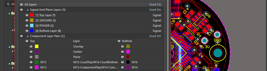
Layers
| Mechanical Layer | Function | Description |
|---|---|---|
| Mechanical 1 | Board outline | PCB outline which can be used to define the board shape. |
| Mechanical 2 | Panel outline | Only used on for panelization to separate the board outlines from the panel outline |
| Mechanical 3 | Case Body | 3D Body for casing and other external interfaces |
| Mechanical 4 | NC Routing | Defines required routing to be performed on a PCB and/or panel |
| Mechanical 7 (pair M8) | Designator Top | Reserved for top when designators cannot be placed on the silkscreen |
| Mechanical 8 (pair M7) | Designator Bottom | Reserved for when designators cannot be placed on the silkscreen |
| Mechanical 13 (pair M14) | Component Top | Top layer component outlines and 3D bodies |
| Mechanical 14 (pair M13) | Component Bottom | Bottom layer component outlines and 3D bodies |
| Mechanical 15 (pair M16) | Courtyard Top | Top layer component courtyard |
| Mechanical 16 (pair M15) | Courtyard Bottom | Bottom layer component courtyard |
Stack up and DRC
- All stackup heights should match your intended PCB
- The stackup should be informed by manufacturer capabilities
- DRC rules should also be informed by manufacturer capabilities
Schematic Library
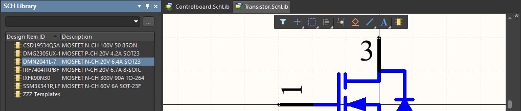
Component designators
| Component | Designator | Component | Designator |
|---|---|---|---|
| BJT | Q? | Jumper | J? |
| Buzzer | B? | LED | D? |
| Capacitor | C? | MOSFET | Q? |
| Capacitor Array | CA? | Motor | M? |
| Chokes | L? | Oscillator | X? |
| Connector | J? | Relay | K? |
| Crystal | X? | Resistor | R? |
| DIAC | D? | Resistor Array | RA? |
| Diode | D? | SIDAC | D? |
| Fan | M? | Solenoid | M? |
| Ferrite Bead | FB? | Speaker | B? |
| Fiducial | FID? | Switch | S? |
| Fuse | F? | Thermistor | R? |
| IC | U? | Transformer | T? |
| Inductor | L? | TVS/Zener | D? |
Each part number has a unique schematic symbol
Keeps the library clean and minimizes accidental build mistakes.
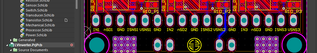
Schematic symbol pins
- When provided, pin numbering shall follow the manufacturer’s datasheet.
- When two row connectors are not given default numbering, zig-zag the numbers down the connector, with odd numbers down one row and even numbers down the opposite row.
- When a part’s pin numbering is ambiguous, number pins counter-clockwise about the component’s center.
- Name the pins the same as the datasheet
Schematic symbol drawing rules
- All symbols use the same color scheme
- Pin designators start at 1, and count up.
- Use a drawing grid of 10 for placing pins.
- Pin size must be a multiple of 10.
| Drawing element | Color | RGB Hex Code |
|---|---|---|
| Pin | black | #000000 |
| Symbol Primitives | blue | #0000FF |
| Box Outline | dark red | #800000 |
| Box Fill | light yellow | #FFFFB0 |
Schematic symbol properties
- Use a component’s part number as the design item ID
- Use Digikey’s descriptions (when possible)
- Include fields for
manufacturer part numberandmanufacturer - Include the following fields:
| Component | Parameter | Description |
|---|---|---|
| BJT | Vce | Max collector-emitter voltage |
| Capacitor/Capacitor Array | Value | Set to capacitance |
| VRating | Capacitor voltage rating |
|
| Crystal/Oscillator | Frequency | Component frequency |
| DIAC/SIDAC | Vbr | Breakover voltage |
| Diode | VReverse | Reverse voltage rating |
| IForward | Maximum forward current |
|
| Ferrite Bead | Value | Set to impedance@freq e.g. 150@10MHz |
| Fuse | IRated | Holding current rating |
| Inductor | Value | Set to inductance |
| IRated | Max or saturation current, whichever is lower |
|
| Mosfet | Vds | Max drain-source voltage |
| Resistor/Resistor Array | Value | Set to resistance |
| Thermistor | RNominal | Nominal resistance at 25°C |
| TVS/Zener | Vz | Zener or breakdown voltage |
Symbol Library Groups
| Library Name | Component Types |
|---|---|
| Capacitor | Capacitor, Capacitor Array |
| Connector | Connector, Jumper |
| Diode | Rectifier Diode, Diode Array, |
| DIAC, SIDAC, | LED, Zener |
| Display | Display IC, Display Modules, LED Modules |
| Filter | Filter IC, Filter module, Ferrite Bead |
| Fuse | Fuse |
| Inductor | Inductor |
| Transistor | N-Channel MOSFET, P-Channel MOSFET, N-Channel JFET, P-Channel JFET,NPN BJT, PNP BJT, IGBTs, SCR, TRIAC |
| Misc | Anything that doesn’t fit elsewhere |
| Oscillator | Crystal, Oscillator, Clock Modules |
| Processor | Microcontroller, Microprocessor, FPGA, Processor Module |
| Protection | TVS Diodes, TVS Modules, Fuses |
| Resistor | Resistor, Resistor Array |
| Sensor | Sensor IC, Sensor Module |
| Switch | Relay, Switch |
| Thermistor | PTC, NTC |
| Transducer | Buzzer, Fan, Motor, Solenoid, Speaker |
| Transformer | Common Mode Chokes, Transformer |
PCB Library
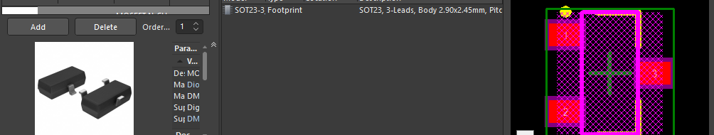
PCB Footprint Drawing
- Pads use the top and/or multilayer
- Silkscreen should be used to show shape and orientation
- Use 0.15mm (6mil) for the minimum silkscreen
- Mechanical layers:
- Layer 13 - Component Body
- Arcs and lines to show shape
- Place 3D bodies here
- Layer 15 - Courtyard
- Arcs and lines of width 0.05mm
- Crosshair of two 1mm long lines to show origin
- Bounding box to assist placement
- Layer 13 - Component Body
- Position 0,0 of the component should be on its center
PCB Footprint Naming
IPC standard chips are named 0803C_N
Use the pattern {imperial package} {type}_{density}.
- {imperial package} is the imperial package (eg. 0402, or 1206).
- {type} is the component type:
- C is capacitor
- D is diode or LED
- F is ferrite bead
- L is inductor
- R is resistor
- {density} is the placement density of the component:
- L is “Least” (or high density)
- N is “Normal” (or medium density)
- M is “Most” (or low density)
IPC standard footprints are named SOIC-8_L
Use the pattern {standard}_{density}
- SOT23-3_M is a “Most” (or low density) SOT23-3 footprint
- SOIC-8_L is a “Least” (or high density) SOIC-8 footprint
Manufacture Specific footprints are named STM_8-DFM-5x6
Use the pattern {manufacturer}_{package}
- SEMTECH_6-QFN is a 16-QFN footprint from SemTech
- STM_8-DFM-5x6 is an 8-DFM footprint from STMicroelectronics
Non-standard footprint naming uses the part number
Use the pattern {partnumber} or {manufacturer}_{partnumber}
Non-component footprint naming is freeform
Footprint library groups
| Library | Footprint Types |
|---|---|
| IPC-Chip | All chip resistors, capacitors etc |
| Mechanical | All non-electonic component footprints, includes mounting, logos, net ties, testpoints, etc. |
| Other IPC | Group all other footprints based on IPC standard, one library per footprint type. e.g. SOT, SOIC etc |
| Non-standard | Group based on component types - same as the symbol library groups |
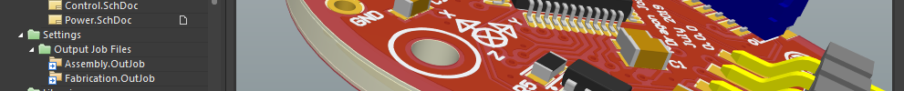
Project Outputs
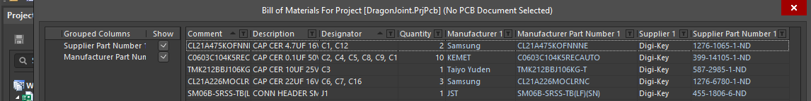
Include the following fields in the bill of materials:
| quantity | designator | comment | description | manufacturer | manufacturer part number |