
Crystal Oscillator Design
Designing good crystal oscillator circuits can be tricky. Most application notes are targeted for mass production; their methods require investing in heavy testing and optimization. This article is for small projects and will help you pick your crystal and capacitors so your circuit will work.
The Circuit Design Process
Four easy steps:
- Select a crystal
- Check that the microcontroller can drive the crystal
- Can the crystal handle the power losses?
- Select load capacitors CL1 and CL2
Step 1: Select a Crystal
You may already have an idea of what kind of crystal you want. Trade-offs between different crystals are discussed later on. Select one which suits your needs but don’t get too attached, we may revisit this step soon.
Step 2: Check That Your Microcontroller Can Drive The Crystal
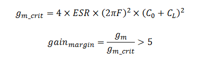
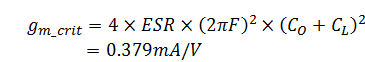
Microcontroller datasheets give some guidance on oscillator selection. These parameters are related to the critical gain. Critical gain is the minimum gain required from the microcontroller circuitry to start the crystal oscillator.
Some microcontroller datasheets provide a set of maximum ESRs allowable from the crystal for a given set of frequencies and load capacitances.
If a microcontroller datasheet provides the oscillator transconductance (usually in uA/V) or a maximum critical gain, then we need to calculate the crystal’s critical gain and check the microcontroller can drive it.
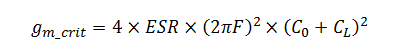
Where:
- F is your crystal’s nominal frequency
- ESR is the crystal’s equivalent series resistance
- C0 is the crystal shunt capacitance
- CL is the crystal’s nominal load capacitance
The critical gain is a property of the crystal, these parameters are in the crystal’s datasheet.
Next calculate the gain margin. If the gain margin is larger than 5, then the oscillator will start up reliably. Larger gain margins mean faster oscillator start up.
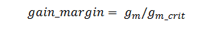
Alternatively some microcontroller datasheets provide a maximum critical gain gm_crit_max. In this case, gm_crit must be less than gm_crit_max.
If the microcontroller does not meet the requirements to drive the crystal, pick another crystal.
Step 3: Can the Crystal Handle the Power Losses?
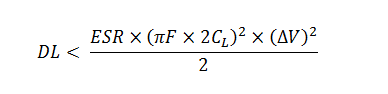
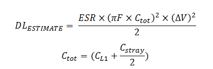
The drive level (DL) of a crystal is specified in the datasheet. The drive level is basically the maximum power rating of the crystal under normal operation.
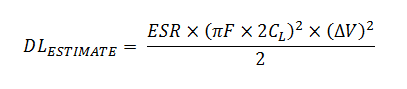
A crude overestimate of the DL can be calculated as follows:

Where:
- ΔV is the peak-to-peak oscillator voltage – use the worst case: ΔV = Vcc
If the estimate is below the crystal’s rated drive level move on to the final step. If the estimate is above the crystal’s rated drive level you can refine the estimate (see an example for this later) or select another crystal and try again.
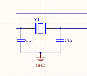
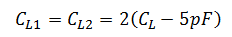
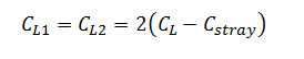
Step 4: Select Load Capacitors CL1 and CL2
The load capacitors tune the crystal to the correct frequency.
The first time I designed a crystal oscillator circuit, I assumed the two load capacitors are connected in parallel. I selected CL1 = CL2 = 0.5*CL. A colleague of mine assumed that CL1 = CL2 = CL. Both of these selections are common. Both are wrong.
The load capacitance is the required capacitance across the crystal, so CL1 and CL2 are connected in series.
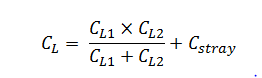
I like to simplify this to:
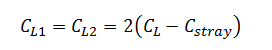
Cstray is the accumulation of stray capacitance from the pins on the microcontroller and trace capacitance. Many application notes recommend estimating this value at about 5pF. Some microcontroller datasheets provide more accurate data on this value – for example, the msp430f22x2 series specifies a stray capacitance of 1pF which fits well with its low-power model. If your microcontroller datasheet doesn’t have this information, estimate Cstray as 5pF.
PCB Design
We want to use the PCB layout to minimize coupling between the oscillator and external signals. High-frequency coupling will excite the upper harmonics of the crystal. The crystal is a source of noise which can interfere with external circuitry.
Rule #1 – Keep the Crystal Close to the Microcontroller
Short traces have low mutual inductance and capacitance. Long traces have high mutual inductance and capacitance. Keeping the crystal close to the microcontroller shortens the traces resulting in less coupling.
Rule #2 – Isolate From High Frquency Signals
When routing non-oscillator signals, keep clear of the oscillator circuitry. This rule applies regardless of which layer you are placing your traces.
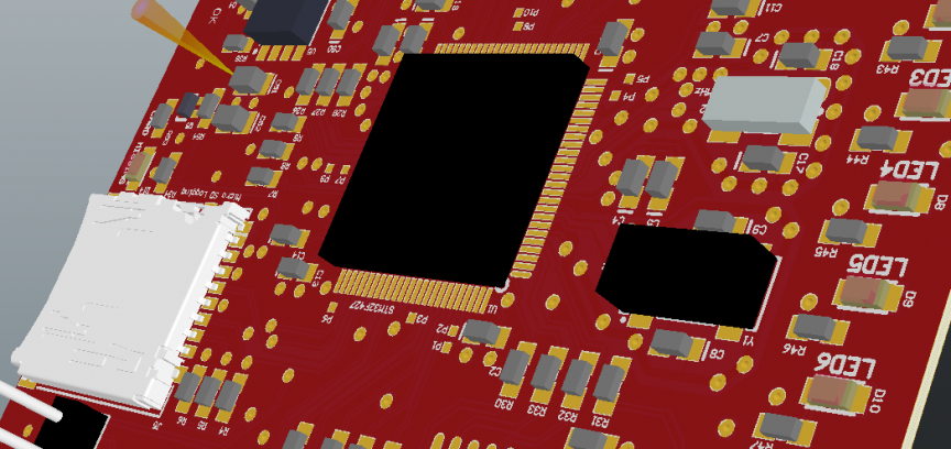
Consider using a guard ring – a copper trace laced with vias which surrounds your oscillator circuit. This will reduce the mutual inductance between external signal lines and the oscillator. Figure 2 shows one I placed in a recent design.
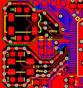
It is common practice to separate the ground plane beneath the oscillator circuit. Connect the separated ground plane at one point at one point only – right next to the microcontroller ground. This prevents return currents from other signal sources from passing through the ground plane used by your oscillator. I have also done this in the design on Figure 2, but it isn’t obvious in the image.
Crystal Selection and Trade-offs
The following trade-offs are made when selecting a crystal: Pullability – a measure of the oscillator’s vulnerability to changes in frequency Power Consumption Start-up time – the time taken to reach stable oscillations after power-up Package size Cost
Trade-off: Pullability versus Power Consumption
Crystals with low pullability require a larger load capacitance. The capacitor energy has to be dumped on each oscillation cycle, so larger load capacitors mean higher power losses. Many microcontroller datasheets recommend a maximum value for load capacitors to reduce the power dissipation in the driving circuitry. So you have a trade-off; robustness or power consumption.
Just to clarify, this trade-off is determined by the CL requirement of the selected crystal; not the CL1 and CL2 values. If power consumption needs to be lowered or pullability improved, select a new crystal requiring a different CL.
Trade-off: Start-up Time versus Package Size
Smaller crystal packages have larger ESRs. Larger ESRs give larger critical gains (gm_crit) lowering the gain margin. A reduced gain margin means the crystal takes longer to start up.
Trade-off: Cost?
As far as I have seen there isn’t a strong correlation between performance and cost. Cost generally comes down to popularity.
Example 1: Desinging an 8MHZ Crystal Oscillator For the STM32
Let’s design an 8MHz crystal oscillator circuit for the STM32F427.
Step 1: Select the Crystal
What tolerance can we have on the crystal?
The STM32F427 datasheet specifies the following:
- for 4-26MHz crystals, Gm_crit_max = 1mA/V
- Frequency tolerance must be +/-500ppm or better
- CL1 and CL2 recommended between 5pF to 25pF each
Let’s select the 7A-8.000MAAJ-T from TXC. The crystal’s small size will allow us to place it close to the STM32 despite the STM32’s 0.5mm pin pitch.
This crystal has the following properties:
- CL = 18pF
- ESR = 60 Ohm
- Frequency Stability = 50ppm
- Frequency Tolerance = 30ppm
- C0 = 7pFmax
- Drive level = 500uW max
Step 2: Check That the Microcontroller Can Drive the Crystal
First, calculate gm_crit:
So gm_crit is below Gm_critmax. The oscillator circuit will start up reliably.
Step 3: Can the Crystal Handle the Power Losses?
Next, roughly estimate the circuitry’s drive level:
= 267uW.
The calculated drive level is below the crystal’s maximum allowable drive level of 500uW.
Step 4: Select Load CapacitorsCL1 and CL2
Assuming Cstray = 5pF (app note AN2867 for the STM32 recommends this as an initial estimate), then:
= 26pF.
The STM32 recommends keeping CL1 and CL2 below 25pF. Suppliers only stock 24pF and 27pF capacitors; 26pF capacitors do not exist. Selecting either 24pF or 27pF capacitors will be fine.
Example #2: Selecting a 16MHZ Crystal Oscillator for the ATMEGA328
This chip seems to be pretty popular. Let’s put a 16MHz crystal on it – just like the Arduino.
Step 1: Select the Crystal
What tolerance can we have on the crystal oscillator?
The ATMega328 datasheet specifies the following:
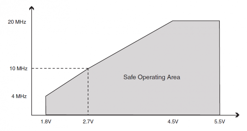
- Minimum voltage for 16MHz is 3.78V to fit in the safe operating are shown in Figure 3. To drive a 16MHz clock, we must at 3.78V or above, for this design we operate at 5V.
- CL1 and CL2 recommended between 12pF to 22pF each
Select the 9B-16.000MAAE-B from TXC.
This crystal has the following properties:
- CL = 12pF
- ESR = 30 Ohm
- Freq Stability = 30ppm
- Frequency Tolerance = 30ppm
- C0 = 7pFmax
- Drive level = 500uW max
Step 2: Check That the Microcontroller Can Drive the Crystal
The ATMega328 doesn’t have a transconductance specification in its datasheet.
You will have to get your embedded developer to set the correct fuses to enable the oscillator once the PCB is populated – this is easily done in Atmel studio.
Step 3: Can the Crystal Handle the Power Losses?
Next, roughly estimate the circuitry’s drive level:
= 545uW.
The drive level estimate is too high. However, we can improve this estimate once we select CL1 and show that the design’s power dissipation is tolerable.
Step 4: Select Load CapacitorsCL1 and CL2
Assuming Cstray = 5pF, then:
= 14pF.
AVX sell a range of 14pF C0G ceramic capacitors suitable for this circuit.
Extra Step: Improve the DL Estimate
From AN2867,
This gives Ctot = 16.5pF and DLESTIMATE = 258uW.
The reason I don’t usually use this equation is that it requires that CL1 is known before checking the drive level. If the drive level from the initial estimate is marginal, you can usually use the above equation to show your crystal selection is suitable.